
Showing posts with label Verilog Codes. Show all posts
Showing posts with label Verilog Codes. Show all posts
Verilog Code for MOD 5 Counter
As discussed in the previous post, I implemented the MOD4 and MOD 8 Counters. In this, I'll implement MOD 5 Counter. This counter will have 5 states starting from 000 to 100 and then again back to zero. However, according to the equation below,
N <= 2n
you might find it vague. I mean 5 is not a power of 2. So how is it possible to design a counter which will count a non-power of 2? If you guessed by using external circuitry, then you are absolutely correct. Within this type of counters, we will have D Flip-Flops with clear flags. By intuition, we can say that just after 100, we will have to somehow clear the flip-flops' values, thus bringing the values back to zero. To calculate the minimum number of gates, we will have to use the same equation. This gives the value of n as 3. Hence, we will have to have 3 D flip-flops to count 5 states in order to satisfy the requirements of MOD 5 counter. Here, we will be using AND gates to clear the flip-flops. OnFor UP counters, we use Q output from each flip-flop. If we assign each bit of 101 to variables A, B, and C then we have to choose only those variables which are HIGH i.e. 1. Here we will choose A and C as both of these variables are 1. Only these variables will act as an input to the AND gate. When the state reaches 5 i.e. 101, AND gate inputs will be 11 which will result in 1 and will be provided to each flip-flop. This will trigger the clear flag within each register, thus will reset each flip-flop to zero and counting of the states will start again.
Pretty Simple huh?
Let us apply the concept to reality.
Our MOD 5 counter will count 5 states i.e. from 0 to 4 and then will reset the flip-flops back to zero. One can make a careful observation that the AND gate that has been used must have some propagation delay. An ideal AND gate would hang the counter onto a single state forever. The proposed counter is an asynchronous counter as each flip-flop is not simultaneously triggered and the clock is depended from the previous flip-flop.
Here is the Verilog code for the implementation:
Here is the output

Carefully Observe that the counter partially goes into the 6th state but resets itself. This delay is because of the AND gate which takes time to compute the result. Here, have a look at the RTL schematic of the MOD 5 Counter.

In the Verilog code, I have introduced a delay of 1ns for the AND gate. Try to set it to 0 and give it a shot. You might think that you would get an ideal MOD 5 counter but it won't happen. The system will hang at 110.
Why does it happen?
Well, it happens because of edge issue. In the Verilog code, observe the always condition. It says @(posedge clk or posedge clear), which means from state 100 as soon the third flip-flop goes from 0 to 1 to make the state 101 at the positive edge of the clock, the AND gate with no delay will also turn on at the same instant. Thus counter stops as it cannot follow the two conditions at the same time. However, giving a delay will first activate the clock condition and then after the delay period arrives the clear edge which will reset the flip-flop again.
Problemo Solved!
I2C Verilog Code and working

I had already made a post regarding I2C long ago, however, in this post I am reposting I2C but with various changes. Some changes involve the using of Acknowledgement Bit by the Slave and Master, Same SDA line for slave address, register address as well as data. No extra data line is required to read the data from the slave. Everything can be seen on the SDA line along. This version of I2C in Verilog has the full support of adding *multiple* slaves.
Yes!! You can use multiple slaves at the same time. The only feature lacking that I am working on right now is the RW bit. The RW or better say Read/Write bit is present here but I have focussed only on the read operation here. I am working on the write operation too and will update soon for the latter.
For this I2C I had to grasp myself with the knowledge of the inout signal line in Xilinx. The SDA has to be an inout line or else it won't be a proper I2C model, despite serving the same functionality.
The Master will send 7-bit address along with RW bit on the SDA line and the corresponding slave will respond back with an ACK bit. After that Master will send the register address which will be acknowledged
by the slave with an ACK bit. Then the slave will send the 8-bit data from the received register to the Master. After receiving the data, Master will respond back with ACK bit and after a CC the I2C operation will end with the STOP bit.
The SCL line changes only when SDA is stable. The testbench I have used here only acts as a supervisor which provides a clock signal to Master. The Master is connected to the slave only with SDA and SCL line.
*DISCLAIMER: This Verilog Code only supports "Read" Operation. I'll continue with the "Write" operation later.
I have worked on this code using a different approach. If the Slave address that Master sends doesn't match with the Slave then it will keep on sending the same address. However, this approach is only applicable to 1 Slave. Consider the case where there are two slaves S1 and S2. If S1 address is matched then data exchange takes place between Master and S1. However, S2 will then inflict as the address won't match here. This will lead to an error on the SDA lines inform of X.
Thus to overcome this difficulty I have re-changed the code to NOT to send address, again and again, i.e if the address doesn't match then Master won't resend the address. Although a Master should keep on sending the address in real, my code faces a problem which I'll deal later.
As I have mentioned that I have used inout command in this code. Inout command should only be used using a tri-state buffer.
A tristate buffer is coded somewhat like this:
x <= direction?data:1'bZ;
A tristate buffer has an enable pin. When enabled (here direction == TRUE) then data will be transmitted. On the other case, when disabled (here direction == FALSE) then a high impedance is
sent thereby disconnecting the output from the input circuit. Consider A and B. When A is true then it is at higher potential. When B is false it is at a lower potential. As current flows from High to Low, this signal will blow from A(TRUE - 1) to B (FALSE Z). Similarly, if B is true and A is false then signal will flow from B to A.
While I was coding, I faced tremendous problems with switching between TRUE and FALSE in both Master and Slave. If both A and B are set to TRUE then you will get ZZZZZZZ (in blue color) as output. If both A and B are low you will get XXXXXX (in red color) as output.
The signal line of type inout can only be a wire. It cannot be registered as reg type so to use it we have to use the "assign" keyword.

RW- 0 ACK = 1 Slave address matched

RW- 0 ACK = 0 Slave address not matched
Get Single Master Single Slave Code from here: Github I2C_Code
Master & Slave
Test Bench
NOTE - To restart the I2C transmission all you have to do is give a fork join condition| fork | |
| #160 alpha <= 0; | |
| #160 direction <= 1; | |
| #162 left_bits <= 1; | |
| join |
Place this piece of code in the initial begin of the Master Code. Remember that you have to give sufficient #time condition to avoid conflict. With this you can you can pull SDA line low to restart I2C for a new data. However, data will too remain the same. Thus you will have to change the data by using #time syntax like this in Master
fork
#160 alpha <= 0;
#160 direction <= 1;
#162 left_bits <= 1;
#160 register = 7'b00011001; // 00011001 = 25 in decimal
#160 reg_temp = register;
join
In Slave you will have to enter new data in the array at location 25.
Sim View of the code above in Xilinx

For Multi Slave I2C significant changes are required. Consider a case where we have two slaves named A and B. The master will send the address of A. In that case slave A will send acknowledgment bit (1 in this case) on the sda line. However, slave B will also send acknowledgment bit (0 in this case). This creates a problem as Verilog doesn't allow multiple drivers for a single wire. Even if I simulated I got ZZ as the acknowledgment because of that conflict.
It can be represented as follows

Thus to avoid this condition I used the Verilog keyword "wor". wor is logical OR of wires joint together.
In case if Slave A NACK = 0 and Slave B NACK = 1 then wor would output as 1(B) + 0(A) = 1
Similarly
0(A) + 0(B) = 0
0(A) + 1(B) = 0
1(A) + 1(B) = NOT POSSIBLE FOR I2C WITH SAME ADDRESS.
The following piece of code has a single master and 3 slaves. One thing I came to notice that all slaves code can remain same except the module name or else any change made to any slave would result in a change is every slave.
Multi Slave Code (Works Pretty well. Comment or message for any error)
To change slave address one can change it to desired address by changing address at line 22 of Master
To fully understand my code click HERE
So Long
I2C Verilog Code and working
I had already made a post regarding I2C long ago, however, in this post I am reposting I2C but with various changes. Some changes involve the using of Acknowledgement Bit by the Slave and Master, Same SDA line for slave address, register address as well as data. No extra data line is required to read the data from the slave. Everything can be seen on the SDA line along. This version of I2C in Verilog has the full support of adding *multiple* slaves.Yes!! You can use multiple slaves at the same time. The only feature lacking that I am working on right now is the RW bit. The RW or better say Read/Write bit is present here but I have focussed only on the read operation here. I am working on the write operation too and will update soon for the latter.
For this I2C I had to grasp myself with the knowledge of the inout signal line in Xilinx. The SDA has to be an inout line or else it won't be a proper I2C model, despite serving the same functionality.
The Master will send 7-bit address along with RW bit on the SDA line and the corresponding slave will respond back with an ACK bit. After that Master will send the register address which will be acknowledged
by the slave with an ACK bit. Then the slave will send the 8-bit data from the received register to the Master. After receiving the data, Master will respond back with ACK bit and after a CC the I2C operation will end with the STOP bit.
The SCL line changes only when SDA is stable. The testbench I have used here only acts as a supervisor which provides a clock signal to Master. The Master is connected to the slave only with SDA and SCL line.
*DISCLAIMER: This Verilog Code only supports "Read" Operation. I'll continue with the "Write" operation later.
I have worked on this code using a different approach. If the Slave address that Master sends doesn't match with the Slave then it will keep on sending the same address. However, this approach is only applicable to 1 Slave. Consider the case where there are two slaves S1 and S2. If S1 address is matched then data exchange takes place between Master and S1. However, S2 will then inflict as the address won't match here. This will lead to an error on the SDA lines inform of X.
Thus to overcome this difficulty I have re-changed the code to NOT to send address, again and again, i.e if the address doesn't match then Master won't resend the address. Although a Master should keep on sending the address in real, my code faces a problem which I'll deal later.
As I have mentioned that I have used inout command in this code. Inout command should only be used using a tri-state buffer.
A tristate buffer is coded somewhat like this:
x <= direction?data:1'bZ;
A tristate buffer has an enable pin. When enabled (here direction == TRUE) then data will be transmitted. On the other case, when disabled (here direction == FALSE) then a high impedance is
sent thereby disconnecting the output from the input circuit. Consider A and B. When A is true then it is at higher potential. When B is false it is at a lower potential. As current flows from High to Low, this signal will blow from A(TRUE - 1) to B (FALSE Z). Similarly, if B is true and A is false then signal will flow from B to A.
sent thereby disconnecting the output from the input circuit. Consider A and B. When A is true then it is at higher potential. When B is false it is at a lower potential. As current flows from High to Low, this signal will blow from A(TRUE - 1) to B (FALSE Z). Similarly, if B is true and A is false then signal will flow from B to A.
While I was coding, I faced tremendous problems with switching between TRUE and FALSE in both Master and Slave. If both A and B are set to TRUE then you will get ZZZZZZZ (in blue color) as output. If both A and B are low you will get XXXXXX (in red color) as output.
RW- 0 ACK = 1 Slave address matched
RW- 0 ACK = 0 Slave address not matched
Get Single Master Single Slave Code from here: Github I2C_Code
Master & Slave
Test Bench
NOTE - To restart the I2C transmission all you have to do is give a fork join condition| fork | |
| #160 alpha <= 0; | |
| #160 direction <= 1; | |
| #162 left_bits <= 1; | |
| join |
Place this piece of code in the initial begin of the Master Code. Remember that you have to give sufficient #time condition to avoid conflict. With this you can you can pull SDA line low to restart I2C for a new data. However, data will too remain same. Thus you will have to change the data by using #time syntax like this in Master
fork
#160 alpha <= 0;
#160 direction <= 1;
#162 left_bits <= 1;
#160 register = 7'b00011001; // 00011001 = 25 in decimal
#160 reg_temp = register;
join
In Slave you will have to enter new data in the array at location 25.
Sim View of the code above in Xilinx
For Multi Slave I2C significant changes are required. Consider a case where we have two slaves named A and B. The master will send the address of A. In that case slave A will send acknowledgment bit (1 in this case) on the sda line. However, slave B will also send acknowledgment bit (0 in this case). This creates a problem as Verilog doesn't allow multiple drivers for a single wire. Even if I simulated I got ZZ as the acknowledgment because of that conflict.
It can be represented as follows
Thus to avoid this condition I used the Verilog keyword "wor". wor is logical OR of wires joint together.
In case if Slave A NACK = 0 and Slave B NACK = 1 then wor would output as 1(B) + 0(A) = 1
Similarly
0(A) + 0(B) = 0
0(A) + 1(B) = 0
1(A) + 1(B) = NOT POSSIBLE FOR I2C WITH SAME ADDRESS.
The following piece of code has a single master and 3 slaves. One thing I came to notice that all slaves code can remain same except the module name or else any change made to any slave would result in a change is every slave.
Multi Slave Code (Works Pretty well. Comment or message for any error)
To change slave address one can change it to desired address by changing address at line 22 of Master
To fully understand my code click HERE
So Long
Verilog Code for VGA Interface
Verilog Code for VGA Interface

VGA (Video Graphics Array) is a connection protocol used for display related activities and actions. It is basically the connection of cables to an output device. VGA are getting replaced by HDMI and micro HDMI cables but are still in use.
A VGA connector pin has 15 connection pins. There are 3 rows with 5 pins each and a VGA adapter has same number of holes with same trapezoidal orientation to fit the VGA cable.
A typical VGA interface runs on 25MHz. Since our FPGAs have 50MHz clock as default like I have on my Basys2, we have to reduce the clock to 25MHz. For that we will have to use clock divider. The frequency of 25Mhz is called pixel clock for a typical 640 X 320 display resolution.
To interface we need to concentrate on some parameters like HS(Horizontal Sync), VS(Vertical Sync), RGB value.
HS,VS ports are of 1 bit each. These are output ports.
RGB is of 8 bits. First 3bits for RED, next 3 bits for GREEN and final 2 bits for BLUE.
Now take an example of writing where we write from left to right and then move back to start of the next line when we reach to the finish of the previous line. So the time taken to move from the end to start is called retrace time.
Look at the image below.
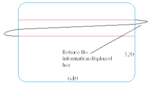
The dimensions are 640 X 320. Image will be displayed where red line is there and not on any retrace area. This retrace time is called “Back Porch”. The retrace at front of display is called “Front Porch”. These porch allow the monitor to jump to next line before drawing since monitor refreshes its screen @60Hz which is pretty slow.
Now to jump and draw on every pixel we must have two counters namely Hcnt and vcnt. HCNT for horizontal pixels counter and VCNT for vertical lines count. The hcnt and vcnt generate the coordinates and according to that coordinates HS and VS signals are switched which allow the circuits to draw an image only in the addressable region.
The pixel clock is the time for display for each pixel. The VS line is the refresh frequency
The HS line starts with H Back Posch area goes forward to H Left Border. You must have seen this border just at the edge of your TV screen. Then follows the H Right Border with H Front Posch.
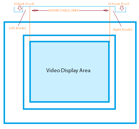
The Hcnt values is 0-96 before H posch back. The H Back Posch with border has 96-144. From 144 to 784 we have addressable area and then 784-799 the rest.
Similarly for vcnt values -2 befor V Posch then 2-35 if for V Posch and border. The addressable region is 35-115 and the rest 515-524.
Remember the drawing area is HCNT – 144 TO 784 and VCNT – 2 to 515(excluded).
Verilog Code for displaying either Red or Green or Blue with switches is below.
Top Module
module testRGB(mlk,r,c,hs,vs);
input mlk;
input [7:0]r;
output [7:0]c;
output hs,vs;
reg clk = 0;
wire [9:0] tc;
always @(posedge mlk)begin
clk = ~clk;
end
main horizontalcounter(clk,rst,hs,vs,r,c);
endmodule
Child Module
module main(clk,rst,qh,vh,r,c);
input clk,rst;
input [7:0] r;
output reg qh;
output reg vh;
output reg [7:0]c;
reg [9:0] hcnt = 0;
reg [9:0] vcnt = 0;
always @(posedge clk)begin
if(hcnt<799 && hcnt>95)
qh <= 1;
else
qh <= 0;
if(hcnt<799)
hcnt <= hcnt + 1;
else
hcnt <= 0;
if(vcnt<524 && vcnt>=2)
vh <= 1;
else
vh <= 0;
if(hcnt==799 && vcnt<524)
vcnt <= vcnt + 1;
if(vcnt>523)
vcnt <= 0;
end
always @(hcnt or vcnt)
if(vcnt>34 && vcnt<515)
if(hcnt>143 && hcnt<784)
c = r;
else
c = 0;
else
c = 8'b0;
endmodule
Test Bench for Top Module
module testbittt;
reg mlk;
reg [7:0] r;
wire [7:0] c;
wire hs;
wire vs;
testRGB uut (
.mlk(mlk),
.r(r),
.c(c),
.hs(hs),
.vs(vs)
);
initial begin
mlk = 0;
end
always #1 mlk = !mlk;
endmodule
The child module will remain inside Top Module. Then make a testbech for the top module.
Here
- r = input from FPGA (8 switches from Baysys2)
- r[7:5] = Reg Color Bits
- r[4:2] = Green Color Bits
- r[1:0] = Blue Color Bits
- qh = HS value. It remains 1 from 95(included) to 799(excluded)
When 799 is attained the HS must tell VCNT to update and jump to next line as it has approached the end.
- vh = VS value. It remains 1 from 2(included) to 524(excluded)
When VCNT has reached 524 then no new lines are available on monitor thus refresh again to starting position i.e. VCNT = 0;
- Addressable area has VCNT from 34(included) to 515(excluded)
- Addressable area has HCNT from 143(included) to 784(excluded).
When within this area the input will be passes to the output visible area else it will remain on the border of screen in non-visible form.
The UCF constrain file has these ports ACCORDING TO BAYSYS2 FPGA and according to the above code.
net "mlk" loc = "B8";
net "r<7>" loc = "N3";
net "r<6>" loc = "E2";
net "r<5>" loc = "F3";
net "r<4>" loc = "G3";
net "r<3>" loc = "B4";
net "r<2>" loc = "K3";
net "r<1>" loc = "L3";
net "r<0>" loc = "P11";
net "hs" loc = "J14";
net "vs" loc = "K13";
net "c<7>" loc = "C14";
net "c<6>" loc = "D13";
net "c<5>" loc = "F13";
net "c<4>" loc = "F14";
net "c<3>" loc = "G13";
net "c<2>" loc = "G14";
net "c<1>" loc = "H13";
net "c<0>" loc = "J13";
Play within the addressable values of HCNT and VCNT to display anything on monitor.
Here is the (child module) code for 4 X 4 chess board
module main(clk,rst,qh,vh,r,c);
input clk,rst;
input [7:0] r;
output reg qh;
output reg vh;
output reg [7:0]c;
reg [9:0] hcnt = 0;
reg [9:0] vcnt = 0;
always @(posedge clk)begin
if(hcnt<799 && hcnt>95)
qh <= 1;
else
qh <= 0;
if(hcnt<799)
hcnt <= hcnt + 1;
else
hcnt <= 0;
if(vcnt<524 && vcnt>=2)
vh <= 1;
else
vh <= 0;
if(hcnt==799 && vcnt<524)
vcnt <= vcnt + 1;
if(vcnt>523)
vcnt <= 0;
end
always @(hcnt or vcnt)
if(vcnt>34 && vcnt<154) if(hcnt>143 && hcnt<263) c = 8'b00000000; else if(hcnt>262 && hcnt<383) c = 8'b11111111; else if(hcnt>382 && hcnt<503) c = 8'b00000000; else if(hcnt>502 && hcnt<623) c = 8'b11111111; else c = 0; else if(vcnt>153 && vcnt<274) if(hcnt>143 && hcnt<263) c = 8'b11111111; else if(hcnt>262 && hcnt<383) c = 8'b00000000; else if(hcnt>382 && hcnt<503) c = 8'b11111111; else if(hcnt>502 && hcnt<623) c = 8'b00000000; else c = 0; else if(vcnt>273 && vcnt<394) if(hcnt>143 && hcnt<263) c = 8'b00000000; else if(hcnt>262 && hcnt<383) c = 8'b11111111; else if(hcnt>382 && hcnt<503) c = 8'b00000000; else if(hcnt>502 && hcnt<623) c = 8'b11111111; else c = 0; else if(vcnt>393 && vcnt<514) if(hcnt>143 && hcnt<263) c = 8'b11111111; else if(hcnt>262 && hcnt<383) c = 8'b00000000; else if(hcnt>382 && hcnt<503) c = 8'b11111111; else if(hcnt>502 && hcnt<623) c = 8'b00000000; else c = 0; else c = 8'b0; endmodule
The top module and testbench remains the same.
Subscribe to:
Posts (Atom)