Verilog Code for VGA Interface

VGA (Video Graphics Array) is a connection protocol used for display related activities and actions. It is basically the connection of cables to an output device. VGA are getting replaced by HDMI and micro HDMI cables but are still in use.
A VGA connector pin has 15 connection pins. There are 3 rows with 5 pins each and a VGA adapter has same number of holes with same trapezoidal orientation to fit the VGA cable.
A typical VGA interface runs on 25MHz. Since our FPGAs have 50MHz clock as default like I have on my Basys2, we have to reduce the clock to 25MHz. For that we will have to use clock divider. The frequency of 25Mhz is called pixel clock for a typical 640 X 320 display resolution.
To interface we need to concentrate on some parameters like HS(Horizontal Sync), VS(Vertical Sync), RGB value.
HS,VS ports are of 1 bit each. These are output ports.
RGB is of 8 bits. First 3bits for RED, next 3 bits for GREEN and final 2 bits for BLUE.
Now take an example of writing where we write from left to right and then move back to start of the next line when we reach to the finish of the previous line. So the time taken to move from the end to start is called retrace time.
Look at the image below.
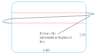
The dimensions are 640 X 320. Image will be displayed where red line is there and not on any retrace area. This retrace time is called “Back Porch”. The retrace at front of display is called “Front Porch”. These porch allow the monitor to jump to next line before drawing since monitor refreshes its screen @60Hz which is pretty slow.
Now to jump and draw on every pixel we must have two counters namely Hcnt and vcnt. HCNT for horizontal pixels counter and VCNT for vertical lines count. The hcnt and vcnt generate the coordinates and according to that coordinates HS and VS signals are switched which allow the circuits to draw an image only in the addressable region.
The pixel clock is the time for display for each pixel. The VS line is the refresh frequency
The HS line starts with H Back Posch area goes forward to H Left Border. You must have seen this border just at the edge of your TV screen. Then follows the H Right Border with H Front Posch.
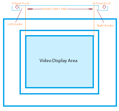
The Hcnt values is 0-96 before H posch back. The H Back Posch with border has 96-144. From 144 to 784 we have addressable area and then 784-799 the rest.
Similarly for vcnt values -2 befor V Posch then 2-35 if for V Posch and border. The addressable region is 35-115 and the rest 515-524.
Remember the drawing area is HCNT – 144 TO 784 and VCNT – 2 to 515(excluded).
Verilog Code for displaying either Red or Green or Blue with switches is below.
Top Module
module testRGB(mlk,r,c,hs,vs);
input mlk;
input [7:0]r;
output [7:0]c;
output hs,vs;
reg clk = 0;
wire [9:0] tc;
always @(posedge mlk)begin
clk = ~clk;
end
main horizontalcounter(clk,rst,hs,vs,r,c);
endmodule
Child Module
module main(clk,rst,qh,vh,r,c);
input clk,rst;
input [7:0] r;
output reg qh;
output reg vh;
output reg [7:0]c;
reg [9:0] hcnt = 0;
reg [9:0] vcnt = 0;
always @(posedge clk)begin
if(hcnt<799 && hcnt>95)
qh <= 1;
else
qh <= 0;
if(hcnt<799)
hcnt <= hcnt + 1;
else
hcnt <= 0;
if(vcnt<524 && vcnt>=2)
vh <= 1;
else
vh <= 0;
if(hcnt==799 && vcnt<524)
vcnt <= vcnt + 1;
if(vcnt>523)
vcnt <= 0;
end
always @(hcnt or vcnt)
if(vcnt>34 && vcnt<515)
if(hcnt>143 && hcnt<784)
c = r;
else
c = 0;
else
c = 8'b0;
endmodule
Test Bench for Top Module
module testbittt;
reg mlk;
reg [7:0] r;
wire [7:0] c;
wire hs;
wire vs;
testRGB uut (
.mlk(mlk),
.r(r),
.c(c),
.hs(hs),
.vs(vs)
);
initial begin
mlk = 0;
end
always #1 mlk = !mlk;
endmodule
The child module will remain inside Top Module. Then make a testbech for the top module.
Here
- r = input from FPGA (8 switches from Baysys2)
- r[7:5] = Reg Color Bits
- r[4:2] = Green Color Bits
- r[1:0] = Blue Color Bits
- qh = HS value. It remains 1 from 95(included) to 799(excluded)
When 799 is attained the HS must tell VCNT to update and jump to next line as it has approached the end.
- vh = VS value. It remains 1 from 2(included) to 524(excluded)
When VCNT has reached 524 then no new lines are available on monitor thus refresh again to starting position i.e. VCNT = 0;
- Addressable area has VCNT from 34(included) to 515(excluded)
- Addressable area has HCNT from 143(included) to 784(excluded).
When within this area the input will be passes to the output visible area else it will remain on the border of screen in non-visible form.
The UCF constrain file has these ports ACCORDING TO BAYSYS2 FPGA and according to the above code.
net "mlk" loc = "B8";
net "r<7>" loc = "N3";
net "r<6>" loc = "E2";
net "r<5>" loc = "F3";
net "r<4>" loc = "G3";
net "r<3>" loc = "B4";
net "r<2>" loc = "K3";
net "r<1>" loc = "L3";
net "r<0>" loc = "P11";
net "hs" loc = "J14";
net "vs" loc = "K13";
net "c<7>" loc = "C14";
net "c<6>" loc = "D13";
net "c<5>" loc = "F13";
net "c<4>" loc = "F14";
net "c<3>" loc = "G13";
net "c<2>" loc = "G14";
net "c<1>" loc = "H13";
net "c<0>" loc = "J13";
Play within the addressable values of HCNT and VCNT to display anything on monitor.
Here is the (child module) code for 4 X 4 chess board
module main(clk,rst,qh,vh,r,c);
input clk,rst;
input [7:0] r;
output reg qh;
output reg vh;
output reg [7:0]c;
reg [9:0] hcnt = 0;
reg [9:0] vcnt = 0;
always @(posedge clk)begin
if(hcnt<799 && hcnt>95)
qh <= 1;
else
qh <= 0;
if(hcnt<799)
hcnt <= hcnt + 1;
else
hcnt <= 0;
if(vcnt<524 && vcnt>=2)
vh <= 1;
else
vh <= 0;
if(hcnt==799 && vcnt<524)
vcnt <= vcnt + 1;
if(vcnt>523)
vcnt <= 0;
end
always @(hcnt or vcnt)
if(vcnt>34 && vcnt<154) if(hcnt>143 && hcnt<263) c = 8'b00000000; else if(hcnt>262 && hcnt<383) c = 8'b11111111; else if(hcnt>382 && hcnt<503) c = 8'b00000000; else if(hcnt>502 && hcnt<623) c = 8'b11111111; else c = 0; else if(vcnt>153 && vcnt<274) if(hcnt>143 && hcnt<263) c = 8'b11111111; else if(hcnt>262 && hcnt<383) c = 8'b00000000; else if(hcnt>382 && hcnt<503) c = 8'b11111111; else if(hcnt>502 && hcnt<623) c = 8'b00000000; else c = 0; else if(vcnt>273 && vcnt<394) if(hcnt>143 && hcnt<263) c = 8'b00000000; else if(hcnt>262 && hcnt<383) c = 8'b11111111; else if(hcnt>382 && hcnt<503) c = 8'b00000000; else if(hcnt>502 && hcnt<623) c = 8'b11111111; else c = 0; else if(vcnt>393 && vcnt<514) if(hcnt>143 && hcnt<263) c = 8'b11111111; else if(hcnt>262 && hcnt<383) c = 8'b00000000; else if(hcnt>382 && hcnt<503) c = 8'b11111111; else if(hcnt>502 && hcnt<623) c = 8'b00000000; else c = 0; else c = 8'b0; endmodule
The top module and testbench remains the same.
No comments:
Post a Comment