SPI Verilog Code

Serial Peripheral Interfacing or simply saying SPI is a communication protocol used between devices to communicate with. They certainly have to talk in the same language or rather say synchronized signals to perform any action.
A particular SPI protocol consists of Microcontroller as Master and another microcontroller or IC as a slave. It is basically a master-slave relationship that exists here. The relationship of SPI can have Multi-master and slaves too. Each master has 4 wire lines at least to communicate with a single slave.
1. The first wire is called the SCL (Serial Clock). Serial Clock works in a tick-tock fashion as soon as the master selects the slave.
2. The second wire is MISO(Master IN Slave Out). This wire acts as an input to the final behavior of the signals sent to the slave. The slave sends the data bit by bit on this line which it synchronizes with the SCL line.
3. The third wire is MOSI (Master Out Slave IN) This wire acts as a carrier which only sends the signals required by the Master to the slave. After analyzing the signal the slave resends the required data back to the master by the MISO line.. The master sends the data bit by bit along this line which is synchronized with the SCL line.
4. The fourth line is the SS (Slave Select) line- This wire is used to select a particular slave. It is proportional to the number of slaves attached to the master. To select a master all the master requires is to pull up the resistor and wire has a value of 1. When not required the resistor is pulled down and wire value is 0.
Working of SPI in a simple explanation
1. First, the Master decides which slave it has to send the signal. Then it will turn the slave select line of that particular slave on i.e. the resistor is pulled down and wire value turns low thereby selecting the slave. As soon as the slave gets selected the wire is still kept low. Remember all slave wires remain high except the one selected i.e. at most one SS will remain low.
2. As soon as the SS turns low the SCL starts ticking the master sends a single bit. This single bit if low will tell the slave that it is a read operation. On the contrary, if this bit is high it will tell the slave that it has to perform the write operation.
3. After sending the read-write bit master starts sending out the address bit by bit on the MOSI line at every posedge of SCL upon which action has to be performed.
4. As soon as the address is finished Master sends out the data in same bit by bit fashion on the MISO line.
5. The slave then writes the data collected at the address sent by the master.
6. If the master sends a read bit then the slave reads the address sent by the master and then passes the require data stored at that particular address bit by bit synchronized with SCL line on the MISO line.
So to clarify all the steps
The SS line is turned down to select the particular slave.

Then as soon as the SS turns down the clock starts ticking a.k.a the SCL line.

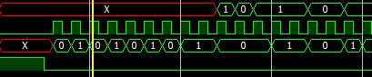
Then with the first positive edge of SCL line read-write bit along with address is sent on the line. The MOSI lines remain null until the SCL line is fired up. The second line diagram after the clock is the MOSI line. Here the first 0 is the read-write bit. Here it is the read bit. The next eight bits are the address bits sent one bit at a time.

Then the data bits are sent one by one. Here we have eight data bits.

So the address bits are 10101011 and the data bits are 00011001 along with the MOSI line.
Just at the moment when the slave receives the address and data bits, it will firstly discard the data bits because it doesn't require it when we have read bit. It will only be used when we have a write bit. So MISO line is turned with data stored at the address sent to the slave. The top line is of MISO which starts as soon as the last bit "1" of the address is received.
Thus the working of SPI is clear as crystal. The Verilog code for the same is down below.
Block Diagram for Single Master and Slave relation.

Output for the SPI code

The above code is only for a single master single slave.

Verilog Code for Multi Slave SPIHere I am sharing the schematic diagram of Multi Slave connection

Verilog Code for MasterSPI
Verilog code for Slave1
Verilog Code for Slave2
Verilog Code for Datapath
Verilog Code for Testbench
This code consists of a single master driving two slaves. Do remember both slaves are different. Both are independent here. Their codes ARE NOT SAME. Many times we same code and instantiate more than once like this.
Slave slv(<inputs><outputs>)
Slave slv2(<inputs><outputs>)
But here each slave has different values or processing and processed values although the mechanism is the same. It is like you have two Arduino where both have the same architecture and working, however, each work for different tasks assigned. If we use the same code then change in one code will change the other too thus arrays and values in it will be the same. Obviously, we do not want that isn't it?
Here is the output for Multi Slave SPI

**Click the image to Magnify**
- The data transfer rate is pretty higher than I2C (Click here).
- No start and stop bits and acknowledge bit like in I2C hence reduced complicated system.
- Both input and output are separate thus can act simultaneously
- Hardware wise it uses four wires while I2C uses two (SDA and SCL).
- No acknowledge bit hence no confirmation from slave.
- Only 1 master is supported.
So Long :)