SPI Verilog Code

Serial Peripheral Interfacing or simply saying SPI is a communication protocol used between devices to communicate with. They certainly have to talk in the same language or rather say synchronized signals to perform any action.
A particular SPI protocol consists of Microcontroller as Master and another microcontroller or IC as a slave. It is basically a master-slave relationship that exists here. The relationship of SPI can have Multi-master and slaves too. Each master has 4 wire lines at least to communicate with a single slave.
1. The first wire is called the SCL (Serial Clock). Serial Clock works in a tick-tock fashion as soon as the master selects the slave.
2. The second wire is MISO(Master IN Slave Out). This wire acts as an input to the final behavior of the signals sent to the slave. The slave sends the data bit by bit on this line which it synchronizes with the SCL line.
3. The third wire is MOSI (Master Out Slave IN) This wire acts as a carrier which only sends the signals required by the Master to the slave. After analyzing the signal the slave resends the required data back to the master by the MISO line.. The master sends the data bit by bit along this line which is synchronized with the SCL line.
4. The fourth line is the SS (Slave Select) line- This wire is used to select a particular slave. It is proportional to the number of slaves attached to the master. To select a master all the master requires is to pull up the resistor and wire has a value of 1. When not required the resistor is pulled down and wire value is 0.
Working of SPI in a simple explanation
1. First, the Master decides which slave it has to send the signal. Then it will turn the slave select line of that particular slave on i.e. the resistor is pulled down and wire value turns low thereby selecting the slave. As soon as the slave gets selected the wire is still kept low. Remember all slave wires remain high except the one selected i.e. at most one SS will remain low.
2. As soon as the SS turns low the SCL starts ticking the master sends a single bit. This single bit if low will tell the slave that it is a read operation. On the contrary, if this bit is high it will tell the slave that it has to perform the write operation.
3. After sending the read-write bit master starts sending out the address bit by bit on the MOSI line at every posedge of SCL upon which action has to be performed.
4. As soon as the address is finished Master sends out the data in same bit by bit fashion on the MISO line.
5. The slave then writes the data collected at the address sent by the master.
6. If the master sends a read bit then the slave reads the address sent by the master and then passes the require data stored at that particular address bit by bit synchronized with SCL line on the MISO line.
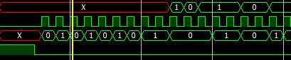
So to clarify all the steps
The SS line is turned down to select the particular slave.

Then as soon as the SS turns down the clock starts ticking a.k.a the SCL line.

Then with the first positive edge of SCL line read-write bit along with address is sent on the line. The MOSI lines remain null until the SCL line is fired up. The second line diagram after the clock is the MOSI line. Here the first 0 is the read-write bit. Here it is the read bit. The next eight bits are the address bits sent one bit at a time.

Then the data bits are sent one by one. Here we have eight data bits.

So the address bits are 10101011 and the data bits are 00011001 along with the MOSI line.
Just at the moment when the slave receives the address and data bits, it will firstly discard the data bits because it doesn't require it when we have read bit. It will only be used when we have a write bit. So MISO line is turned with data stored at the address sent to the slave. The top line is of MISO which starts as soon as the last bit "1" of the address is received.
Thus the working of SPI is clear as crystal. The Verilog code for the same is down below.
Block Diagram for Single Master and Slave relation.

Output for the SPI code

The above code is only for a single master single slave.

Verilog Code for Multi Slave SPIHere I am sharing the schematic diagram of Multi Slave connection

Verilog Code for MasterSPI
Verilog code for Slave1
Verilog Code for Slave2
Verilog Code for Datapath
Verilog Code for Testbench
This code consists of a single master driving two slaves. Do remember both slaves are different. Both are independent here. Their codes ARE NOT SAME. Many times we same code and instantiate more than once like this.
Slave slv(<inputs><outputs>)
Slave slv2(<inputs><outputs>)
But here each slave has different values or processing and processed values although the mechanism is the same. It is like you have two Arduino where both have the same architecture and working, however, each work for different tasks assigned. If we use the same code then change in one code will change the other too thus arrays and values in it will be the same. Obviously, we do not want that isn't it?
Here is the output for Multi Slave SPI

**Click the image to Magnify**
- The data transfer rate is pretty higher than I2C (Click here).
- No start and stop bits and acknowledge bit like in I2C hence reduced complicated system.
- Both input and output are separate thus can act simultaneously
- Hardware wise it uses four wires while I2C uses two (SDA and SCL).
- No acknowledge bit hence no confirmation from slave.
- Only 1 master is supported.
So Long :)
Well how can we connect more slaves. Code for others ?
ReplyDeleteAs I said mechanism is same for each slave. So copy the code of any slave for the new BUT the array where numbers are stored will be different. THIS ARRAY is the difference between every slave as each has different data within them.
Deleteaddress <= {address,mosi};
ReplyDeleteWhat is the meaning of above syntax (in SLAVE code) and why is 'ione' variable used in the code for SLAVE?
address <= {address,mosi};
ReplyDeleteWhat is the meaning of above statement and also why is 'ione' used in the SLAVE code?
ione is counter. Author has used variable i in previous slave code hence I guess he used i1
DeleteFor every tick 1 bit will be passed. Total address will be of 8 bits. So {x,y} concatenates x and y.
ReplyDeleteInitially address is XXXXXXXX. After 1 CCycle it will be XXXXXXXX concatenated with 1 bit mosi.
Assuming address passed on MOSI is 10101010 Thus
address <= {address,mosi}; will yield this
XXXXXXX1 in 1st CC
XXXXXX10 in 2nd CC
XXXXX101 in 3rd CC
XXXX1010 in 4th CC and so on
Shashi,
ReplyDeleteI'm kind of lazy. Is there an easy way to get an Acrobat PDF of your writeup?
Please let me know. Thanks!
Hey Jesse, Sorry but I use cloud services for posts and compiling code hence pdf version isn't available from my side. If you are using an Apple product then you can export this page as .pdf in iBooks. In case you are using Android or Windows based browser, you can use online services to convert webpage to pdf. However in that case, code scripting may get lost.
Deletewhat is meaning of slock in code?
ReplyDeleteSlock is the name of a task. The purpose of slock i.e. task is to execute scl line. If you have used C or C++ then you must be familiar with functions. It works in a similar way.
Deletehi i m subramanian i need the complete output of multiple slave concept without any markings to verify the operation
ReplyDeleteyou can send it to subramanian2828@gmail.com
ReplyDeleteI am getting error for the line Slave1 slv1(scl,miso,mosi,ss1);
ReplyDeleteThe error is :
Invalid use of input signal as target.
I am using xilinx ise 8.1i
ReplyDeleteCan somebody please point out whats wrong. If I remove the line Slave1 slv1(scl,miso,mosi,ss1); the code is compiled but i am not getting the same rtl schematic as u have got(Master and slave both connected). I am getting the schematic for master only
ReplyDeleteThe line that you're removing has a task that is to instantiate the Slave module and join it with Master with correct ports. Since you are removing the line of code that instantiates and joins Slave to Master, it won't show in RTL view as it is not connected at all.
Delete++ Xilinx version has nothing to do with it
++ Invalid use of I/P signal as target means that you must have messed up the ports while instantiating the Slave. Order of ports is very important if you are instantiating a module from a module. If you are doing it from a test bench that it is OK but I haven't used test bench instantiation here.
Even if i copy paste the above code posted for a single slave it gives me the same error :
ReplyDeleteInvalid use of I/P signal as target
RTL Schematic will not allow certain syntax as they cannot be synthesized on an FPGA.
DeleteExample
repeat command
using edge and latch in always block like this
always @(posedge scl or mosi)
Either it will be edge driven or level driven but not both on an FPGA however, on a simulation it is important to see its working.
Although I tried again but didn't get the error as you got.
I am posting the code that has COMMENTED parts to avoid synthesis errors. Uncomment and simulation can be done easily.
MASTER
Deletemodule Master(scl,mosi,miso,ss1,ss2,sel);
output reg scl;
input miso;
output reg [0:0]mosi;
output reg ss1;
output reg ss2;
output reg [1:0] sel;
reg [16:0]xx;
initial begin
scl = 0;
ss1 = 1;
ss2 = 1;
#10 ss1 = 0;
sel = 0;
xx = 17'b011101001_00011001;
#100 ss2 = 0;
xx = 17'b010101011_00011001;
ss1 = 1;
sel = 1;
end
//always @(negedge ss1 or negedge ss2)
//slock ;
always @(posedge scl)begin
mosi = xx[16];
xx = xx<<1;
end
/*task slock;
repeat (38)
#2 scl <= !scl;
endtask: slock;*/
endmodule
SLAVE
Deletemodule Slave1(clk,miso,mosi,ss);
input clk;
input [0:0]mosi;
input ss;
output reg[0:0]miso;
reg [7:0] address,data;reg x1;
reg [7:0] arr [0:309];
reg k;
reg [6:0] i=0;
initial begin
arr[233]=185;
end
always @(mosi or ss)begin
if(i==0 && ss==0)begin
x1 <= mosi;
end
end
always @(posedge clk /*or mosi*/)begin
if(ss==0)begin
//******ADDRESS READ***//
if(i>0 && i<9)begin
address <= {address,mosi};
end
//******DATA READING****//
if(i>8 && i<17 && x1==1)begin
data <= {data,mosi};
end
//*********DATA SENDING TO MASTER MISO***//
else if(i>8 && i<17 && x1==0)begin
miso <= arr[address][7];
arr[address]<=arr[address]<<1;
end
if(i==17)
miso<=1'bz;
//******DATA RECEIVED WRITTEN IN TO THE ADDRESS***//
i<=i+1;
if(i>16 && x1==1)
arr[address]<=data;
end
end
endmodule
DATAPATH
Deletemodule Datapath(miso,mosi,scl,ss1,ss2);
output [0:0]miso;
output [0:0]mosi;
output ss1,ss2,scl;
wire [0:0]miso1,miso2;
wire [1:0]sel;
Master Mas(scl,mosi,miso,ss1,ss2,sel);
Mux mul(miso1,miso2,miso,sel);
Slave1 slv1(scl,miso1,mosi,ss1);
Slave2 slv2(scl,miso2,mosi,ss2);
endmodule
Checked and worked for RTL view as well as simulation.
DeleteEnjoy
Hello. I have to implement an SPI interface between FPGA(Nexys 2 Spartan 3E) and 2 different sensors. In that case, I understand that I have to implement both modules of Slave1 and Slave2. Can I use properly the codes from the last comments? I work with Xilinx
ReplyDeleteHello,
DeleteFor simulation on Xilinx it will definitely work. However, it may not work when implementing on an FPGA because some syntax are not supported by FPGA/RTL
So, for a code working both in FPGA and Xilinx where do you recommend to look for an answer? What should I search for a good implementation?
ReplyDeleteThank you!
You can search on opencores.
DeleteYou can even edit this code as this code is simulation ready but only needs few changes to make it FPGA ready.
Mr.Sashi my doubt is why did you use a task to instantitate clock scl there a simple repeat loop is sufficient in master code ?
ReplyDeleteand my other doubt is what is reg k doing in slave code
is it just copying everything and pasting in order or any kind of manipulation to be done
ReplyDeleteThe first step is learning each line of code.
DeleteThe second step is copying the code and checking it on your own.
Should I copy paste both master and slave modules in a single verilog file or different for single slave implementation? Also is datapath also necessary for it?
ReplyDeleteIn a different Verilog file.
DeleteYes datapath is necessary. It tells about the connection between individual components/modules
nice question mr.jafar khan
DeleteWhere should the data path be given ?
DeleteJust like another verilog module.
DeleteThis comment has been removed by the author.
ReplyDeleteim a beginner i know nothing of verilog tryna learn
ReplyDeletecan u tell me how to implement in xilinx im using rtl
Well Verilog is not that difficult. Do you have a grip on Digital electronics?
DeleteAlso no need to go to RTL right now. One must clear basics first and then implement simple programs first. Success of one project will give confidence to start the second. For now just focus on small code and its compilation without any error.
Ya but I've chose this as project so I need to know how to simulate this
DeleteI need a reply please
DeleteSorry for late reply, I am extremely busy right now. However, that doesn't mean I won't help you. I will soon post a new article about simulation on Xilinx from testbench to datapath along with explanation. Within a week, I'll post it. Hope you can wait.
DeleteVisit this post. It might help you
Deletehttps://www.hellocodings.com/2018/12/how-to-simulate-verilog-code-in-xilinx.html
How many module to be created how does test bench be given
ReplyDeleteI will soon post a new article about simulation on Xilinx from testbench to datapath along with explanation. Within a week, I'll post it. Hope you can wait.
DeleteVisit this post
Deletehttps://www.hellocodings.com/2018/12/how-to-simulate-verilog-code-in-xilinx.html